Do we delve deeply enough into the actual physical mechanism of current flow through electrical conductors using the concepts of charge carriers and electric fields in our treatments for GCSE and A-level Physics? I must reluctantly admit that I am increasingly of the opinion that the answer is no.
In part one we discussed two common misconceptions about the physical mechanism of current flow, namely:
- The all-the-electrons-in-a-conductor-repel-each-other misconception; and
- The electric-field-of-the-battery-makes-all-the-charge-carriers-in-the-circuit-move misconception.
What, then, does produce the internal electric field that drives charge carriers through a conductor?
Let’s begin by looking at the properties that such a field should have.
Current and electric field in an ohmic conductor

(You can see a more rigorous derivation of this result in Duffin 1980: 161.)
We can see that if we consider an ohmic conductor then for a current flow of uniform current density J we need a uniform electric field E acting in the same direction as J.
What produces the electric field inside a current-carrying conductor?
The electric field that drives charge carriers through a conductor is produced by a gradient of surface charge on the outside of the conductor.

Rings of equal charge density (and the same sign) contribute zero electric field at a location midway between the two rings, whereas rings of unequal charge density (or different sign) contribute a non-zero field at that location.
Sherwood and Chabay (1999): 9
These rings of surface charge produce not only an internal field Enet as shown, but also external fields than can, under the right circumstances, be detected.
Relationship between surface charge densities and the internal electric field
Picture a large capacity parallel plate capacitor discharging through a length of high resistance wire of uniform cross section so that the capacitor takes a long time to discharge. We will consider a significant period of time (a small fraction of RC) when the circuit is in a quasi-steady state with a current density of constant magnitude J. Since E = J / σ then the internal electric field Enet produced by the rings of surface charge must be as shown below.
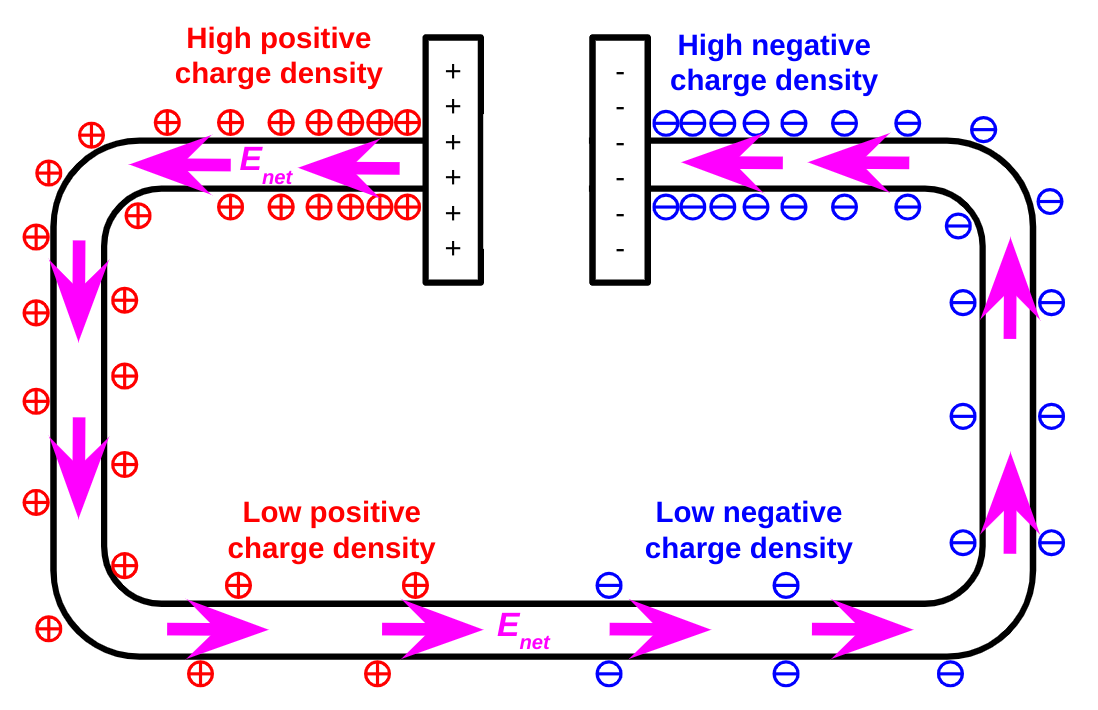
In essence, the electric field of the battery polarises the conducting material of the circuit producing a non-uniform arrangement of surface charges. The pattern of surface charges produces an electric field of constant magnitude Enet which drives a current density of constant magnitude J through the circuit.
As Duffin (1980: 167) puts it:
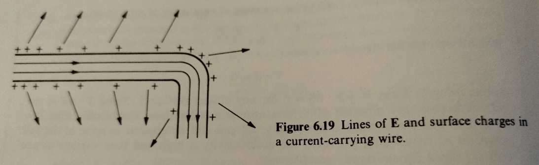
Granted that the currents flowing in wires containing no electromotances [EMFs] are produced by electric fields due to charges, how is it that such a field can follow the tortuous meanderings of typical networks? […] Figure 6.19 shows diagrammatically (1) how a charge density which decreases slowly along the surface of a wire produces an internal E-field along the wire and (2) how a slight excess charge on one side can bend the field into the new direction. Rosser (1970) has shown that no more than an odd electron is needed to bend E around a ninety degree corner in a typical wire.
Rosser suggests that for a current of one amp flowing in a copper wire of cross sectional area of one square millimetre the required charge distribution for a 90 degree turn is 6 x 10⁻³ positive ions per cm3 which they call a “minute charge distribution”.
Observing the internal and external electric fields of a current carrying conductor
Jefimenko (1962) commented that at the time
no generally known methods for demonstrating the structure of the electric field of the current-carrying conductors appear to exist, and the diagrams of these fields can usually be found only in the highly specialized literature. This […] frequently causes the student to remain virtually ignorant of the structure and properties of the electric field inside and, especially, outside the current-carrying conductors of even the simplest geometry.
Jefimenko developed a technique involving transparent conductive ink on glass plates and grass seeds (similar to the classic linear Nuffield A-level Physics electrostatic practical!) to show the internal and external electric field lines associated with current-carrying conductors. Dry grass seeds “line up” with electric field lines in a manner analogous to iron filings and magnetic field lines.

Next post
In part 3, we will analyse the transient processes by which these surface charge distributions are set up.
References
Duffin, W. J. (1980). Electricity and magnetism (3rd ed.). McGraw Hill Book Co.
Jefimenko, O. (1962). Demonstration of the electric fields of current-carrying conductors. American Journal of Physics, 30(1), 19-21.
Rosser, W. G. V. (1970). Magnitudes of surface charge distributions associated with electric current flow. American Journal of Physics, 38(2), 265-266.
Sherwood, B. A., & Chabay, R. W. (1999). A unified treatment of electrostatics and circuits. URL http://cil. andrew. cmu. edu/emi. (Note: this article is dated as 2009 on Google Scholar but the text is internally dated as 1999)